Q&A for PCB service
If there is any question, please feel free to email PCB@elecrow.com, we will reply soon.
1 layer 2layer 4layer PCB quotation online https://www.elecrow.com/pcb-manufacturing.html?utm_source=wiki&utm_medium=pcb
For special needs PCB fabrication, PCB assembly, Mechanical Service/Molding/laser cutting etc needs. please feel free to contact service@elecrow.com
Q&A For PCB Service
- Q: I used the CAM file on your website, why there isn't drill layer in the gerber file?
- A: Display all the layers before you exporting the gerber file from the eagle file to have a try. The format of the drill file can be excellon or RS-274x format And the drill file is solid circle with size when checked by gerber viewer.
-
Ps: there are many customers send the gerber file without the drill file. The drill file in the gerber file should be solid hole with size.
-
Q: Is there a way to provide the information regarding non-plated through holes to you in future designs?
- A: We will plate all the holes by default. If you need some holes not be plated, please name the plated holes/via layer as PCBname-PHT.txt and name the non-plated holes layer as PCBname-NPTH.txt.
-
PS: For holes display on the GML/GKO layer, we will fabricated as Non-plated default. If need to fabricate as plated holes, please leave a comment.
-
Q: What the dielectric constant is for your PCBs?
-
A: This is the datasheet of the material of FR4 http://www.elecrow.com/wiki/images/3/34/PCB_material_FR-4_info.pdf
-
Q: Boards are outline milled, right?
- A: Yes, The outline and all the GML layer will be milled or add V-groove following the lines. The V-cut line can be added on the GML/GKO layer.
The tolerance of outline is ±0.2mm from the middle of the outline.
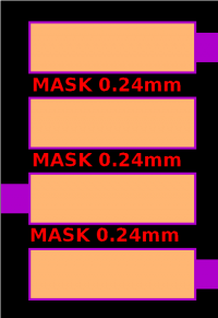
- Q: What the minimum space to print the solder mask between the IC pads. is the following picture ok?
- A: Sorry, It is not ok to print the solder mask. The minimum space to print the solder mask is 0.3mm. For less than 0.3mm spacing, we won't print the solder mask between the pads.
You can leave a comment for this so that our engineer will contact you if we can't print the solder mask between the IC pads.
- Q: What's the recommend space between two sub-PCB with V-groove.
- A: The minimum distance between the copper/trace and the V-groove line is 0.4mm/16mil.
And the minimum distance between the board outline GML/GKO layer and the copper/ trace is 0.3mm/12mil.
- Q: Are blind and buried vias supported?
- A: Blind vias are not available for normal PCB service. It is ok to fabricate blind/buried vias for premium PCB service
The following picture show the difference between buried via, blind via and Through hole. Through holes is ok for fabrication by the normal PCB service.

- Q: Is it possible to repeat a previous order? If you have saved the gerber file of course.
-
A: It is ok to repeat a previous order. You can leave a comment for the previous order number and file number on Elecrow website and gerber file name.
-
Q: What the minimum space or slot in the PCB can you fabricate?
-
A: The diameter of the milling cutter is 0.8mm. So the minimum space or slot is 1mm.
-
Q: How far away do I need the silkscreen/traces from the board outline?
-
A: The minimum distance is 0.3mm.
-
Q: For the PCB rush service, It says rush 12 hours, why it is 2 to 3 working days.
-
A: We will ship out PCB in 2 days normally. But there is weekend each week and the customers is from worldwide, We don't make sure that we can arrange it into fabrication immediately.
-
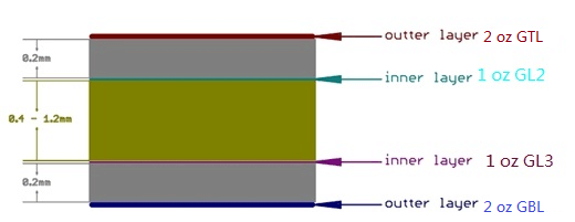
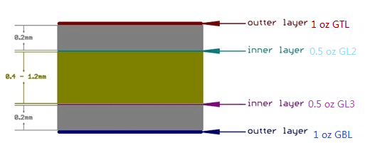
Q: What is the stack up for your 4 layers pcb?
- A: Please look at the following picture and mark the layers as GTL, GL2, GL3 and GBL.The thickness of the inner layer is 1oz now.Please note, the outer layer thickness is not the unique value(0.2mm) for normal PCB service.
Please contact us for inquiring if you have strict requirements for the layer stack up.
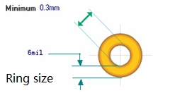
- Q: What is the minimum recommended annular ring size for your 2 layer (color free) service?
- A: Please have a look at the following picture.
- Q: what is the minimum gap between a via and a route ?
-
A: The minimum gap between a via and a route is 6mil.
-
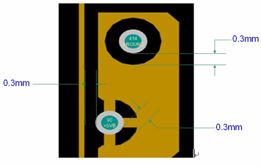
Q:What the recommend minimum space between the THT pad and copper?
- A: The recommend minimum distance is 0.3mm to avoid circuit short when soldering.
- Q:What is the minimum space between holes? To make sure, see this picture;
-
A: The minimum of W1 is 0.45mm. there is no request about W2.
-
Q: Do you offer silkscreen for free on both layers?
- A: silkscreen for both side is free. There are black and white two silkscreen color.
Solder mask for both side is free too. There are six option color: Green, Red, Blue, Yellow, Black and White. Matte green and Matte black needs $20 extra fabrication fees.
- Q: What the minimum distance between two panelized PCBs?
-
A: Zero distance is recommend.
- ps1: The milling cutter can only run straight line. And the V-groove straight line should through the whole board.
- ps2: For larger quantities (over 200pcs), we will combine your PCBs automatically to a panel.If you donot want it or want to define your own panel, please leave a comment.
-
Q: What is minimum width of silkscreen printing?
- A: Minimum height 40mil is recommend, 32 mil is also ok. Please have a look at the following picture.
- Q: Can you please provide a list of available drill sizes for the prototype PCB service?
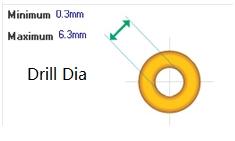
- A: The drill size is 0.3mm, 0.35mm, 0.4mm, 0.45mm etc.to 6.0mm. it is 0.05mm increments to 6.0mm.
The PCB engineer will enlarge the PCB drill file about 0.15mm for Hasl finished PCB and enlarge 0.1mm for the ENIG finished PCB to ensure the finished drill size is almost the same as the design.
- Q: What is maximum PCB size? 20cm x 20cm?
- A: The maximum PCB size that our normal PCB service can manufacturing is 60*60cm.
For PCB less than 30*30cm, you can order it on the website. For PCB larger than 30*30cm, you can send the gerber file and parameter( qty, color, thickness, surface finished) to service@elecrow.com. we will give the quotation to you soon. For small batch of PCB fabrication, You can order the PCB via the PCB area.
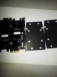
- Q: Is two design sub-board allowed? (Two design PCB is separated by V-groove)
-
A: Yes, it is ok now, you can order it online.
-
Q: Is “custom shape” allowed? (see following pictures)
- A: Yes, All is ok. The space between the outline needs to larger than 1mm.
The following PCB designed by Sparkfun may for your reference. This shape looks great.
- Q: Do you provide "castellated via" and how can I do that.
- A: Yes, Castellated via is ok for fabrication. You can cut the hole by GKO/GML and leave a comment that you need these hole to be castellated via(Plated half Holes).
It needs $16 extra fees. You can purchase 16 units of Premium PCB service(SKU: PRE88740PCB)when place the order online and leave a comment. If these Half hole don't need to be plated, it doesn't need extra fees. It may need more extra fees if the board is complex or have many castellated holes and we will contact you before fabrication.
- Q: For the premium pcb service, can I use the matte black?
- A: The green and black color use the matte black and matte Green. The price is a little higher than normal solder mask color.
- Q: Does the small batch of PCB support urgent process?
-
A: The e-test time for small batch of PCB fabrication is much more than prototyping PCBs(5pcs, 10pcs and 20pcs). So the lead time for small batch of PCB fabrication needs to more than 2 days at least.
-
Q: My CAD software, KiCAD, does not create NC drill.txt and mechanical layer.GML. What the mechanical layer it is? Is is ok without these files?
- A: The mechanical layer.GML is PCB outline file. It can placed on other layers. If the gerber file is RS-274x format and all the needed file is included, it should be ok for fabrication.
