


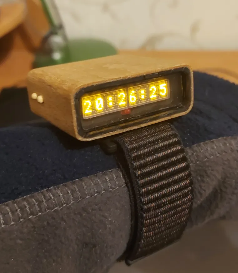
Story
Choosing the microcontoller
When I was planing the entire project I also decided to make it more challenging and interesting to me. And because of that chose a bit unusual MCU for this watches. My pick stick to ATtiny85 - I beleived that it would be an interesting challenge to make watch on this MC, but later I had to switch to ATtiny85 and I will describe why so. Most basic MC for such project would be ATmega328, which is used in Arduino UNO, but again, it was not interesting enough to me and the solution on this MC is already exist on the net.
Another reason why I’ve chosen AVR MCU but not ARM (STM32) or other is because I’ve already had enough knowledge and skills about programming such MCUs.
So, as you probably know, ATtiny85 has not a lot of pins, actually there are only 5 pins which I could use to run an entire watch! It means that I had to design various drivers and multiplexers to drive all the devices with which ATtiny communicates.
Display driver
The key devices which are driven by MCU are of course indicators HDSP-2000, without them entire project has no any sense. Due to the lack of available pins in MCU, display driver should receive data from a small amount of pins. If we look closer at the indicator, we’ll see that it is basically a shift register which receives data through SPI bus. It can be inferred, that the most vital signals for indicator are serial clock and serial data signals. All other signals can be generated from clock and data signals and I will explain how.
First of all, let’s have a look at columns signals. Each time a high voltage level is applied to one of these pins the corresponding columns in LED matrix are driven and the LEDs in this column emit light. It means that after the new values have been stored to the shift registers the next column should be driven. Basically, it is very similar to the “running leds” projects, which can be easily built on decimal counters like CD4017. Each time a new data is stored to the shift registers of indicators, the counter CD4017 will count to the next value and the corresponding output pin will drive the column of indicator. Schematic of indicator is shown on fig. 1.

Figure 1. - HDSP-2000 indicator schematic
Another problem is to get know when the transition of data to shift registers is finished. This issue also can be solved with counters. By counting the number of bits, which were transferred, it can be checked whether or not the process is finished. In HDSP-2000 there are four shift registers and each of them stores 7 bits, so the total data capacity of indicator is 28 bits. Since two indicators are used in this project, the capacity of display block is twice bigger, which is 56 bits. The amount of bits which were sent to the display can be obtained from serial clock signal – each positive front of clock represents a one bit of data that has been stored to the indicator. To count bits a binary 7-stage counter CD4024 was used. The binary representation of decimal number 56 is 111000, so the corresponding pins Q3, Q4, and Q5 are high when counter reach value 56. Early mentioned pins are tied to single AND gate with 3 inputs. Output signal of AND gate is used as clock signal for decimal counter CD4017. Drivers schematic is shown on fig. 2.

Figure 2. - Display driver schematic
Since indicator HDSP-2000 has only 5 columns counter CD4017 counts only from value 1 to 5. When counter reaches value 5, corresponding pin “5” changes its state from low to high and through RC low-pass filter sets high level on signal RST while simultaneously driving fifth column of indicator. When high level is set on RST pin of counter it resets its value. RC low-pass filter is needed to create a time delay, so the fifth column could be driven for some consistent time. The same solution was used to the output of AND gate in order make sure that positive clock front for decimal counter CD4017 would not disappear instantly after binary counter CD4024 resets. The signal from AND gate is also used to bias current mirrors in indicators which basically enables LEDs in indicator to emit light. By changing resistance and capacitance in the RC filter it is possible to regulate the width of pulses that AND gate produces. Consequently it will make LEDs in indicator to “glow” for longer or lesser amount of time which mean that it is possible to regulate a brightness of the display. Timing diagram for the signals described above is shown on fig. 3.

Figure 3. - Timing diagram of signals in display driver
Bipolar PNP transistors were used in order to provide a current for the each column of the indicator. Since the low level signal is required to open bipolar transistor and decimal counter can provide only high level signal for each output pin it was decoded to use inverter on N-channel MOS transistors.
Supply core
Supply core circuit (fig. 4) consists of the next blocks:
-
Accumulator;
-
Charging circuit;
-
DC-DC step up converter;
-
Linear voltage regulator;
-
Resistive divider of accumulator voltage;

Figure 4. - Supply core schematic
Li-Po accumulator was chosen as a voltage source because of the next advantages: it is rechargeable, it could be found in various sizes rather than Li-Ion cells. The output voltage of li-po accumulator is in range from 2.7 to 4.2 while all electronic components consume voltage of 3.3 V. To provide 3.3 V for all components a linear regulator XC6206 was used. This regulator delivers 3.3 V on its out when voltage on its input is higher than 3.4 V.
To monitor whether or not voltage on accumulator dropped to 3.4 V a resistive divider was used. Voltage between two resistors is applied to one of the pins of MC where it is then converted to binary code by ADC. When display shows that battery charge is 0% it means that voltage on accumulator is about 3.4 V, so the watch should be charged. Diode VD3 and capacitor C8 form a pic detector. Such a detector is needed due to voltage drop of accumulator when indicators are turned on.
The main part of charging circuit is LTC4054 – a programmable linear charger. Circuit itself is pretty simple: resistor R19 sets the charging current which in this case is about 200 mA; LED HL1 indicates whether or not battery has charged – when LED is on it means that the battery is not full, when LED is off – battery is fully charged. Supply voltage for this IC is 5 V which is delivered from USB. More information about how does this circuit works can be found in datasheet for this IC.
DC-DC step-up converter is used in this watch to power HDSP indicators since they require 5 V for proper operation while maximum voltage level on battery can reach only 4.2 V. Circuit of this step-up converter was taken from the datasheet for the IC that is used in this converter which is SX1308. There will not be any explanation of how does this step-up converter work since this is not the main aim but it is worth mention the purpose of transistor VT11. This transistor is needed to disconnect battery from converter when indicators are not used in order to reduce power consumption of the watch when they are turned off.
Control core
Control core (fig. 5) consists of the following blocks:
-
MC ATtiny 85;
-
Multiplexers;
-
Real time clock;
-
HDSP indicators;
-
Voltage shifters;
-
Buttons;

Figure 5. - Control core schematic
The main processing unit of the entire watch is microcontroller ATtiny 85. In total only two pins are required to run indicators, four to program MC and other two to communicate with RTC. Those pins are PB2 (SCK / SCL), PB1 (MISO), PB0 (MOSI / SDA) and PB5 (RESET). HDSP-2000 indicators use SPI bus to transfer data so pins PB1 and PB2 are used to send data to the indicators. RTC DS1337 use I2C bus to exchange data with MC and because of that it was decided to use pins PB2 and PB0 to communicate with MC. The last one group of pins is used to program MC through UART interface. To do so signal pins PB0, PB1, PB2 and PB5 should be connected to the programming device. Since all the devices that are connected to those pins cannot be connected together with each other simultaneously due to data collisions it is better to multiplex all the signals in different moments of time.
Signals multiplexing
First of all it is better to establish function of switching between programming mode and operating mode. This task is solved by usage of analog multiplexer DD8 (CD4053) which has three 1 to 2 multiplexers. It was decided to use analog multiplexers because data is being transferred in both direction. When LOW level is present on pins A, B and C of multiplexer pins ax, bx and cx are tied to az, bz and cz respectively. In this case watch operates in showing time mode and pins PB0, PB1 and PB2 are connected to periphery (indicators, RTC, buttons). When HIGH level is applied to multiplexer’s control pins outputs ay, by and cy are tied to input pins az, bz and cz which means that watch is operating in programming mode and pins PB0, PB1 and PB2 are connected to programming port XS7. Switching between modes is done by external switch SW3.
Pin ax of DD8 is used to transfer clock signal CLK_BUS from MC to HDSP indicators and RTC. Because indicators and RTC use different buses it is better to multiplex clock signal so the clock inputs of both indicators and RTC will be isolated from each other. To do so multiplexer DD9 (CD4053) is used. Pin bx of DD8 is used to transfer serial data to indicators. Since indicators operate on 5V shifters DD5 and DD6 are used to convert 3.3V D_OUT and SCLK signals to 5V signals. Pin cx of DD8 is used to exchange data between MC and RTC via I2C bus. Pins bx and by are used to measure buttons state and battery voltage level and pins ax and ay are used to drive MOS transistor VT11 in supply core.
Buttons control and battery voltage measurement
Since MC Attiny 85 has limited amount of pins that can be used as inputs for buttons signals, it is way more convenient to represent signals from multiple buttons as different voltage levels. It can be accomplished by voltage dividers. In supply core there are two buttons: SW1 and SW2. If voltage level on net Buttons is equal to 0V it means that SW1 is pressed, if level is higher than 0V – SW2 is pressed. Note that such configuration of voltage divider and buttons does not support multiple press on both button because in this case voltage level on the net still will be 0V. Later voltage level on the net is measured by builtin ADC in microcontroller and converted to digital code. By comparing the ADC output code it can be figured out which button is pressed.
Voltage level of battery is measured via voltage divider R20-R23 in supply core, since its voltage can reach values of 4.2V while maximum operating voltage of MC is 3.3V. Voltage divider provides only half of battery voltage, so it is safer for ADC to measure it. Also voltage from battery is applied to resistive divider R20-R23 through peak detector VD3-C8. Peak detector is needed because battery voltage drops when load is applied to it, like DC-DC step-up converter for indicators.
Finally, diode VD2 and integrator C7-R32 are used to keep DC-DC boost converter active while data is being sent to indicators. Without this solution text on display would blink.
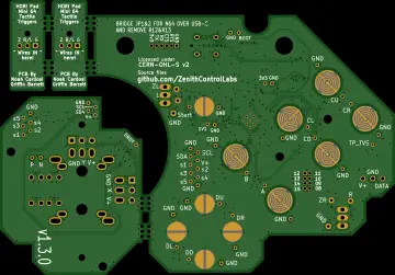
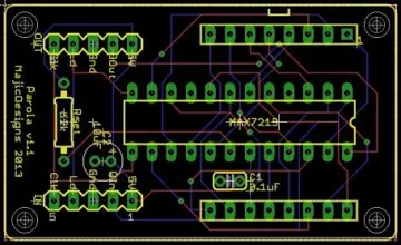
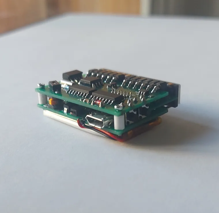
PCB Design
All PCBs and schematics were designed in Altium designed V20. At first I tried to make PCBs by myself but after I got them I realized that its quality is not satisfying. After that I assumed that it would be better to order my PCBs from a company that specializes in its manufacturing. My ordered PCBs that I got from this shop are shown below.