Story
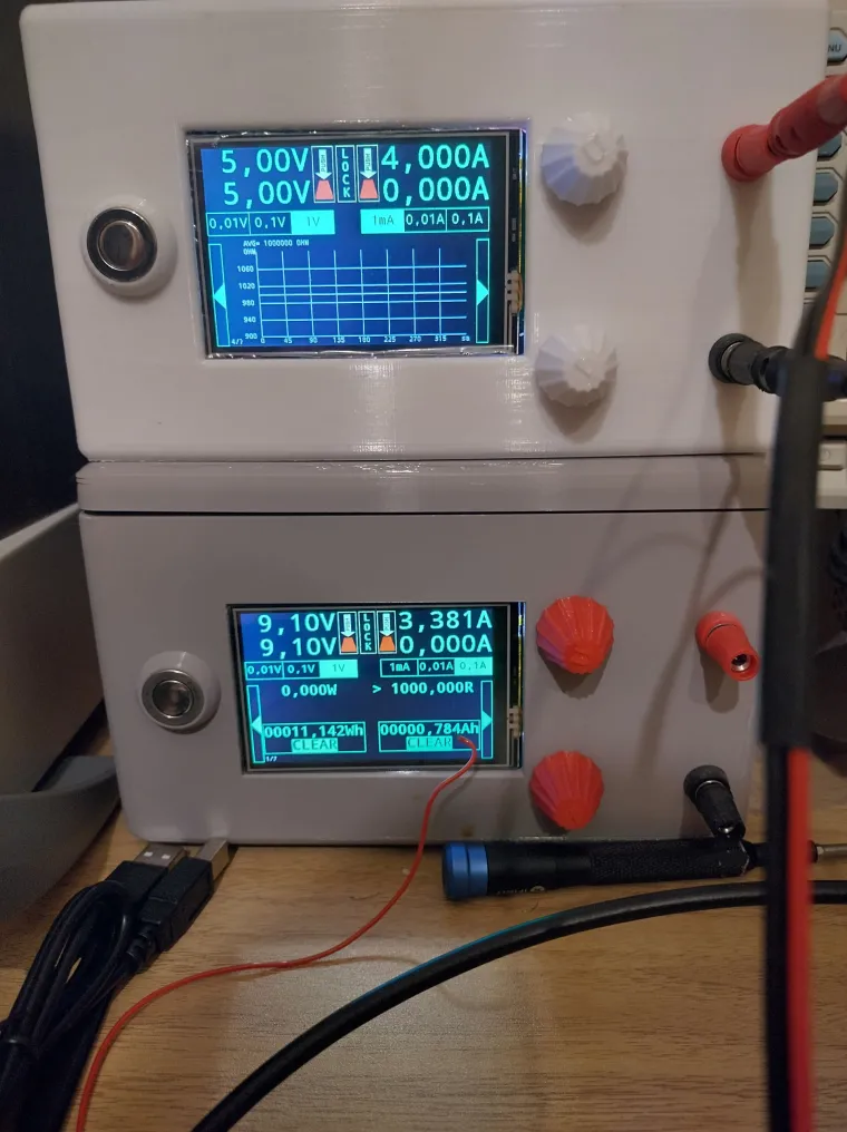
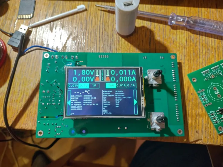
My power supply allows for setting both voltage and current limits using rotary encoders, features a 3.5" touchscreen LCD display, and offers remote control via a 2.4GHz RFM75 module (the same one I used in my Energy meter project). Voltage can be adjusted within a 0-35V range, and the current limit from 0-7A. The adjustment step for voltage and current can be set on the display – 10mV, 100mV, 1V for voltage, and 1mA, 10mA, 100mA for current.
In addition to voltage and current, the display shows load resistance, power consumption, charge in ampere-hours, and energy in watt-hours. Measured data can also be displayed in graph format.
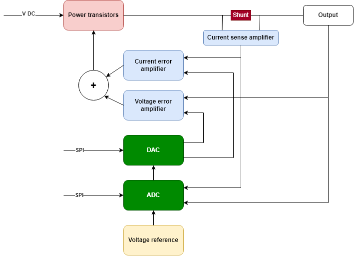
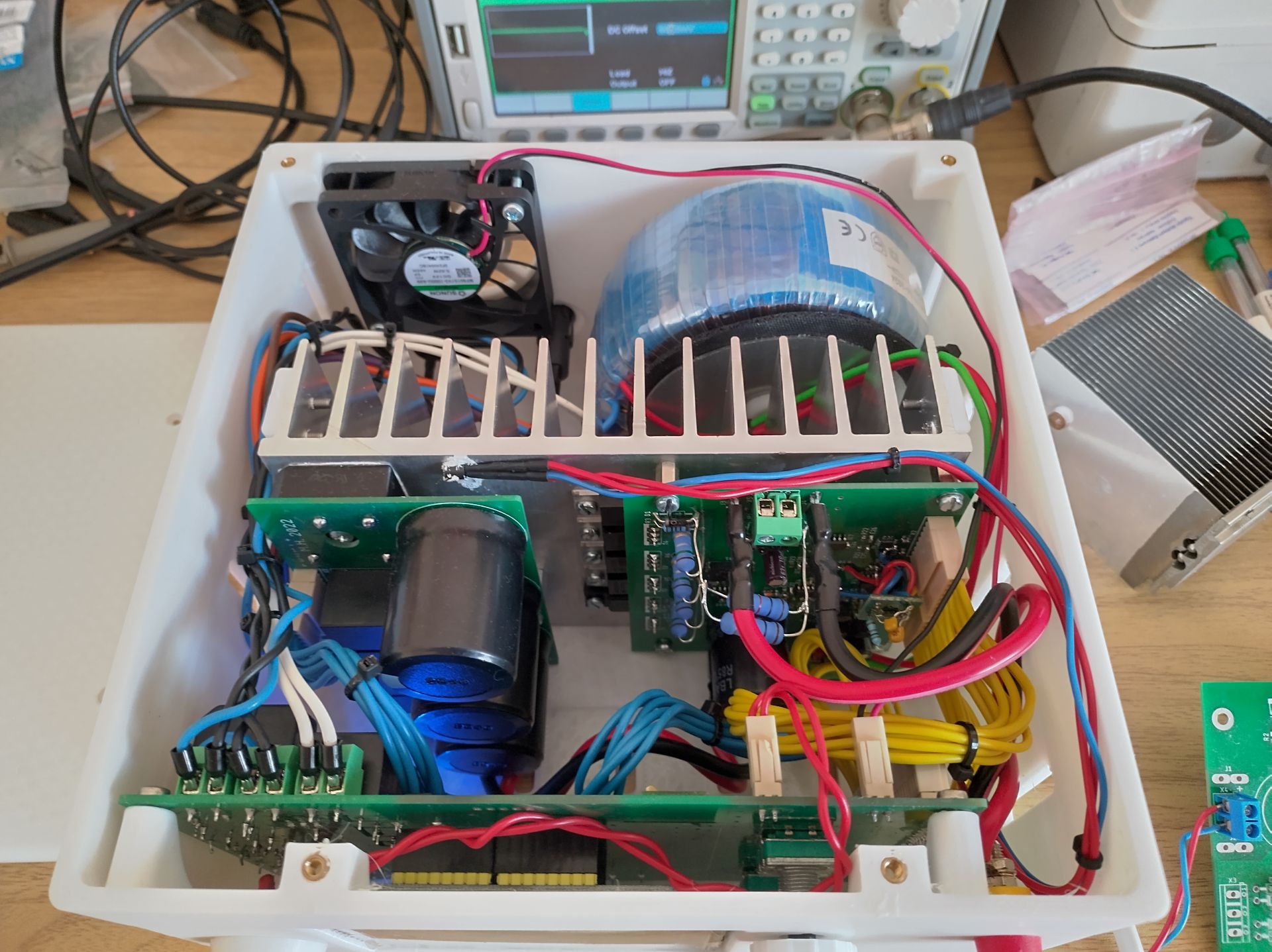
The power supply comprises a toroidal transformer and three PCBs, with their functions illustrated in a simplified block diagram.

From a circuitry standpoint, the power supply is designed as a linear analog system with two control loops regulated by a 16-bit DAC AD5663 (initially, a 12-bit DAC LTC2632 was used, and the new DAC is wired in). A 16-bit ADC LTC1865 is used to measure voltage and current. Both the ADC and DAC communicate with the MCU via an optically isolated SPI bus. As error amplifiers, I used OPA140 operational amplifiers, whose outputs are merged through diodes to control MJE15030A power transistors in a Darlington configuration with BDW93 and BC846. To minimize thermal losses on the transistors, a toroidal transformer with four windings was used, which switches according to the set output voltage.
The output current is measured as the voltage drop across a 10-milliohm resistor, which is further amplified by an OPA228 operational amplifier with a gain of 50. An IC REF5040, providing a 4.096V output, is used as the voltage reference for both ADC and DAC.
The power supply is controlled by a PIC32MM0256GPM028 microcontroller, with firmware written entirely in C (including graphic libraries) in the MPLAB X environment. Eagle CAD was used for PCB design, and the enclosure was created in Fusion 360.

Schematics
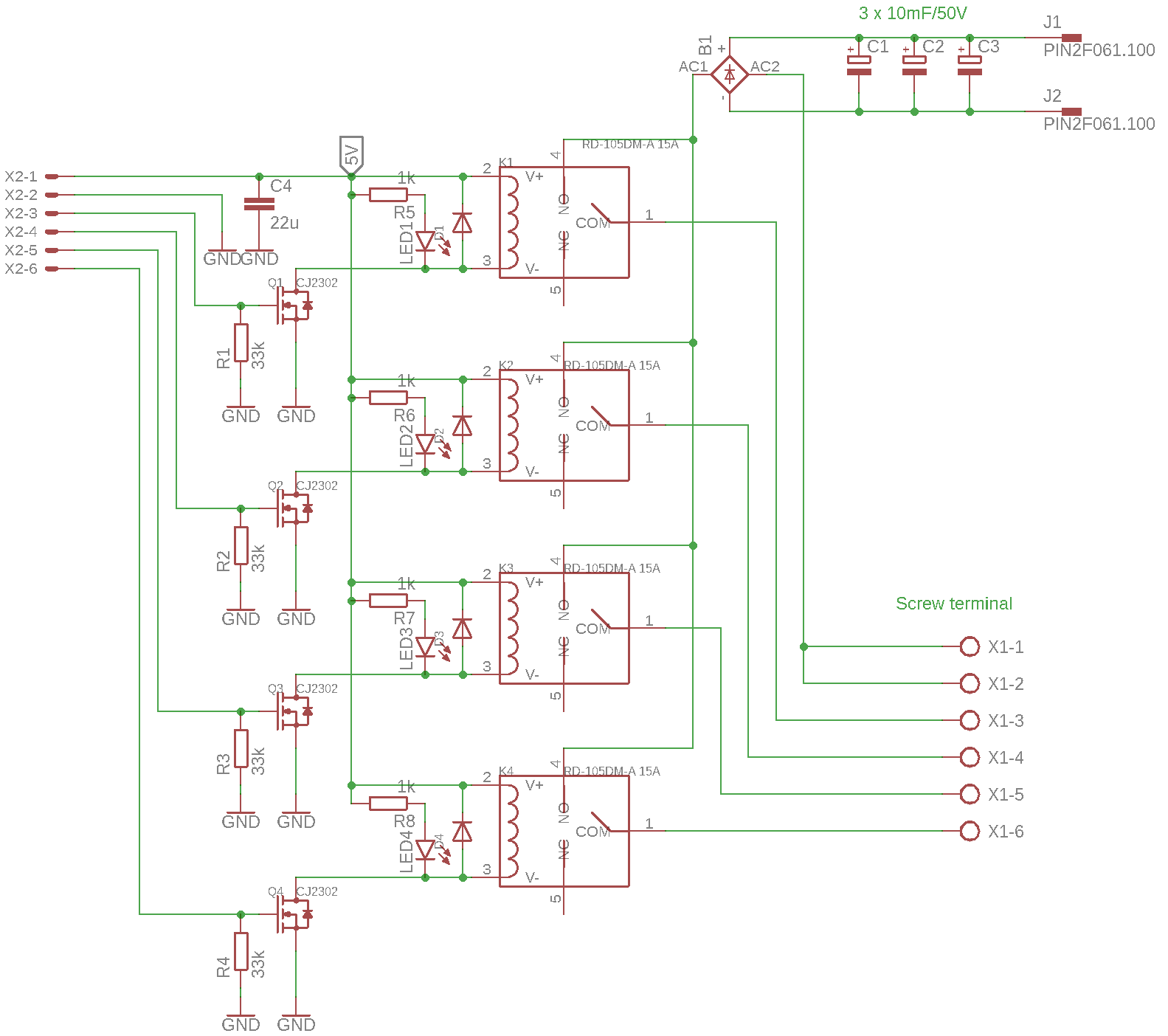
Rectifier, capacitors and transformer tap switches (PCB 3)
Analog control circuits of power supply (PCB 2)

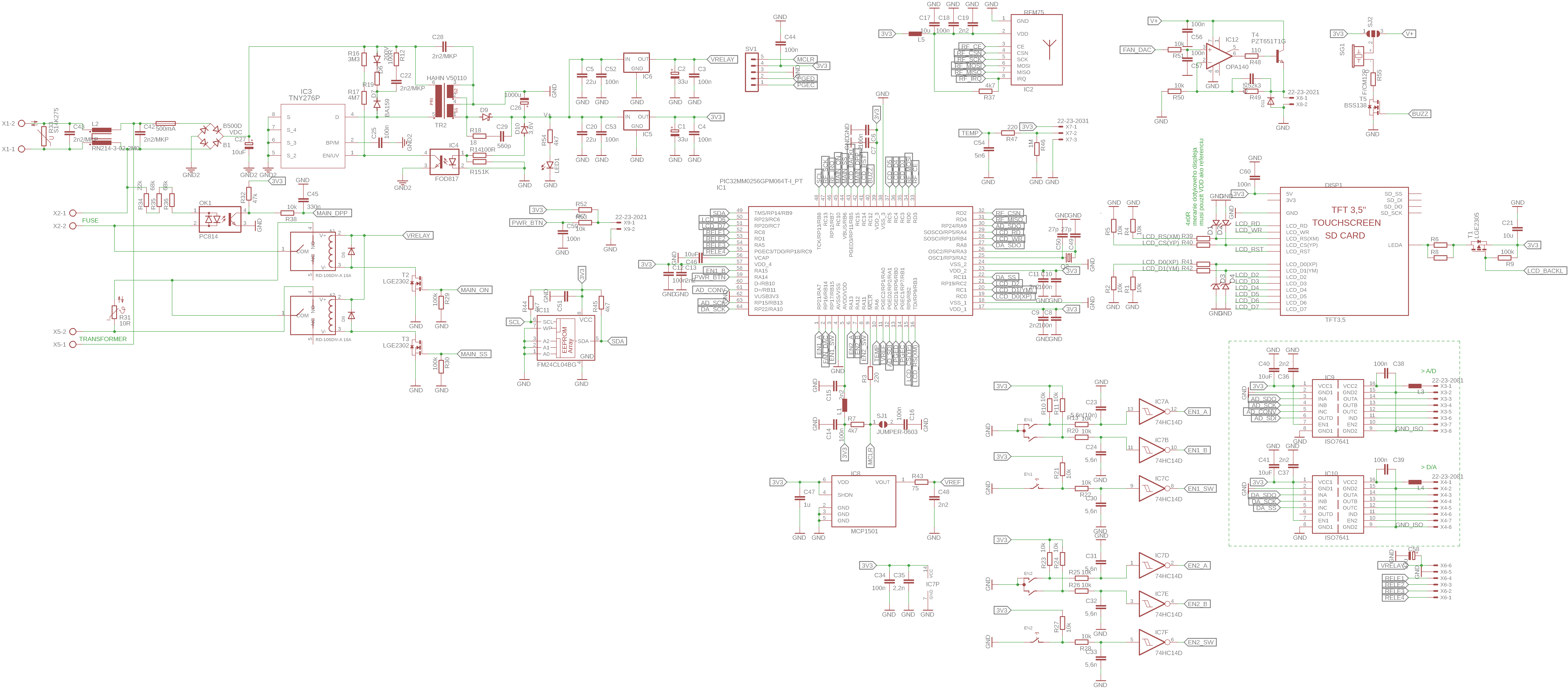
Main board schematics (PCB 1)
Measurements
I did some measurements to verify the dynamic properties of the power supply.
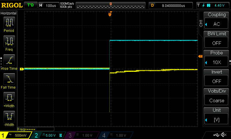
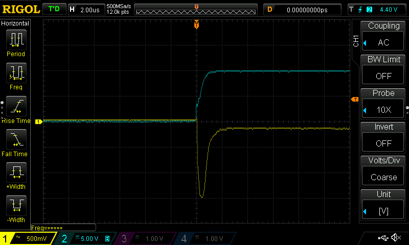
First, i measured the transient step load response in CV mode. Output voltage was set to 10V, load resistance was 5 Ohms switched by MOSFETs.
(Yellow trace is the output voltage. Blue trace is the gate control signal)
CV - 10Vout, 5R load, ON
CV - 10Vout, 5R load, ON, zoomedCV - 5Vout, 5R load, OFF, zoomed
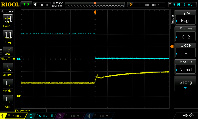
Transition from CV to CC (and vice versa). Output voltage was to 10V, current limit to 1A and the load resistance was 5 Ohms.

from CC back to CV
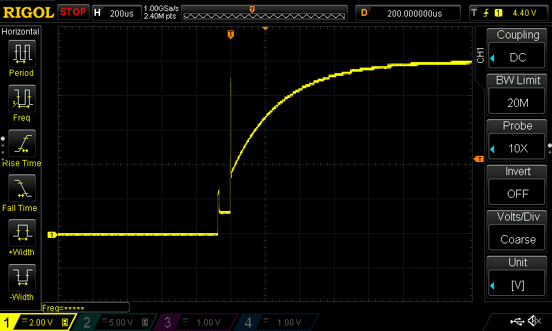
Voltage rise after power-up
