Jumperlux Kit With RGB LEDs
- Buy 5 for $54.40 each and save 15%
- Buy 10 for $52.00 each and save 19%
Does it bug anyone else that microcontroller boards take up most of the space on a breadboard?
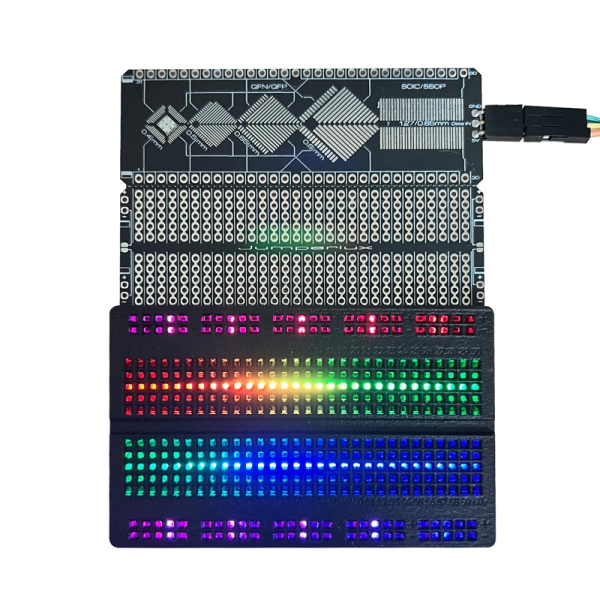
Well, it does for me. So I figured since I was already making custom breadboards for a different project, Jumperless, I should make a simple, passive version that brings a protoboard out on the top with each row connected to the corresponding row on the breadboard. And after doing that, I might as well put some universal SMD pads and have those connect to the breadboard too.
If you don't want any of those things, you can snap them off into 3 separate parts and use each independently.
LEDs
The breadboards optionally have 80 WS2812C-2020-V1 addressable RGB LEDs under each row, with connections for the data and power in a few places, and a data out so these can be chained together and driven by one microcontroller.
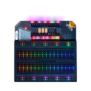
Note that there's no built-in microcontroller to drive the LEDs, but it's trivial to solder any microcontroller you like onto the SMD breakout and run a jumper to the LED data in and use the Adafruit Neopixel library to control them.
If you have a Raspberry Pi Pico, you can use the Jumperless firmware and the Jumperless Wokwi Bridge app to have the LEDs automatically show the connections on whatever circuit you make on Wokwi as soon as you hit save in your browser.
SMD Breakout
The SMD pads support a pretty broad range of SMD chips in various pitches:
- 0.4mm QFN/QFP 32-48 (this was made to support an RP2040)
- 0.5mm QFN/QFP 12-56
- 0.65mm QFN/QFP 12-56
- 0.8mm QFN/QFP 12-56
- 1.27mm SOIC 1-30
- 0.65mm SOIC 1-60
For larger chips you'll probably need to tape off the ground pad on the bottom of the chip so they don't short everything, that's just kind of the nature of universal SMD pads.
Mapping a variable number of SMD pads from a square chip is a weird problem, what I decided to do was have each of the 4 sides mapped to 4 parts on the breadboard. The footprints are at 45 degrees, so if you just imagine squishing the square chip flat, and having the left side start at 1 and the right side of the corner start at breadboard row 16 (or 46 for the bottom), it should kind of make sense.
That was the least confusing way I could come up with, so there are also guides on the silkscreen.
Solderable Protoboard
The protoboard area is way more straightforward, just mapped 1 to 1 with the breadboard. The power rails are off to the sides with little pictures to show which ones they are. There's also a little solder jumper to connect the top and bottom rails together because I always forget to do that and wonder why my circuit doesn't work.
Also note that this is **not** a Jumperless, there are no crosspoint switches making connections for you, so you'll need to use regular jumpers like a cave person. It's my fault for making the names so similar, but I came up with it right when I finished routing the traces and my brain was a bit fried.
If you want be a cool future person and use a jumperless breadboard, the Jumperless is over here


 United States
