Currency
Toggle Nav

What Is A PCB Stencil And How To Use It?
January 18, 2022
What is a PCB Stencil?
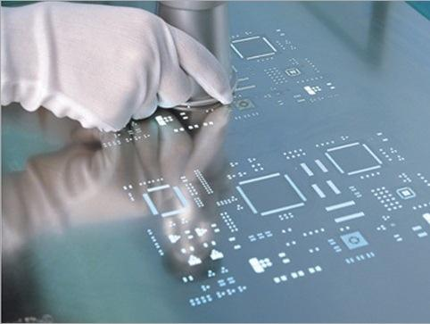
PCB Stencil, also known as Steel mesh, Its main function is to help solder paste deposition and transfer an accurate amount of solder paste to an accurate position on the bare PCB. The stencil is composed of stencil frame, wire mesh and steel sheet. There are many holes in the stencil, and the positions of these holes correspond to the positions that need to be printed on the PCB. When in use, place the PCB under the stencil, he solder paste is leaked to the PCB through the small hole at the fixed position on the stencil. The less solder paste is blocked on the stencil, the more it is deposited on the PCB. Therefore, when there is any defect in the printing process, the condition of the stencil should be checked first.
What is a PCB Stencil made of?
1.Stencil frame
The stencil frame is divided into movable frame and fixed frame. The movable frame directly installs the steel sheet on the frame, and one stencil frame can be used repeatedly; fixed frame is to stick the wire mesh on the stencil frame with glue, The fixed frame is easy to obtain uniform steel sheet tension, which is generally 35 ~ 48N / cm2. (the allowable tension of normal fixed frame is 35 N- 42 N).
2.Mesh
Mesh is used to fix steel sheet and stencil frame. It can be divided into stainless steel mesh and polymer polyester mesh. Stainless steel wire mesh is usually about 100 mesh, which can provide stable and sufficient tension. However, after using for a long time, the stainless steel wire mesh is easy to deform and lose tension; Polyester mesh fly organic matter which is not easy to deform and has a long service life.
3.Sheet
There are copper sheet, stainless steel sheet, nickel alloy, polyester, etc. The stencil generally adopts foreign high-quality 301 / 304 stainless steel sheet, which greatly improves the service life of the stencil with its excellent mechanical properties.
4.Glue
The glue used to paste the mesh frame and steel sheet plays a great role in the stencil. It can be used according to the different customers. This glue can maintain firm adhesion and resist the complex cleaning of various stencil cleaning agents.
Manufacturing Method of Stencil
PCB Stencil can be divided into seven types: laser stencil, electropolishing stencil, electroforming stencil, step stencil, bonding stencil, nickel plating stencil and etching stencil. There are three methods for manufacturing SMT stencil: chemical etching, laser cutting and electroforming. Because Elecrow generally uses laser stencil, the following focuses on laser stencil and laser cutting method. The data file required to make the laser stencil must contain SMT solder paste layer, fiducial mark data, PCB outline layer and character layer, so we can check the front and back sides of the data, component category, etc.
Laser stencil
Laser stencil is the most commonly used in SMT industry, which is characterized is:
The data file is directly used to reduce the manufacturing error;
The opening position accuracy of SMT stencil is extremely high: the whole process error is ≤± 4 μ m;
The opening of SMT stencil has geometry, which is conducive to the printing and molding of solder paste.
Laser cutting
Process flow: film making PCB → taking coordinates → data file → data processing → laser cutting → grinding → Stencil.
Features: high data production accuracy and little influence of objective factors; Trapezoidal opening is conducive to demoulding, It can be used for precision cutting, price cheapness.
General requirements and principles of PCB Stencil
1.The specific position and specification shall ensure high opening accuracy, and the opening shall be in strict accordance with the specified opening method.
2.The independent opening specification shall not be too large, and the total width shall not exceed 2mm. A 0.4mm bridge shall be erected in the middle of the pad specification exceeding 2mm to prevent affecting the strength of the stencil.
3.When stretching the mesh, strictly control it, and pay special attention to the opening range, which must be horizontal and centered.
4.With the printing surface as the top, the lower opening of the mesh shall be 0.01mm or 0.02mm wider than the upper opening, that is, the opening shall be inverted conical to facilitate the effective release of solder paste and reduce the cleaning times of the stencil.
5.The mesh wall must be smooth. Especially for QFP and CSP with spacing less than 0.5mm, the supplier is required to conduct electropolishing during the manufacturing process.
6.Generally, the stencil opening specification and shape of SMT components are consistent with the pad, and the opening ratio is 1:1.
How to design a PCB Stencil?
1.0805 package is recommended to cut the two pads of the opening by 1.0mm, and then make the concave circle B = 2 / 5Y; A = 0.25mm or a = 2 / 5 * l anti tin bead.
2.Chip 1206 and above: after the two pads are moved outward by 0.1mm respectively, make an inner concave circle B = 2 / 5Y; A = 2 / 5 * l anti tin bead treatment.
3.For PCB with BGA, the opening ratio of stencil with ball spacing of more than 1.0mm is 1:1, and the opening ratio of stencil with ball spacing of less than 0.5mm is 1:0.95.
4.For all QFP and SOP with 0.5mm pitch, the opening ratio in the total width direction is 1:0.8.
5.The opening ratio in the length direction is 1:1.1, with 0.4mm pitch QFP, the opening in the total width direction is 1:0.8, the opening in the length direction is 1:1.1, and the outer rounding foot. Chamfer radius r = 0.12mm. The total opening width of SOP element with 0.65mm pitch is reduced by 10%.
6.When PLCC32 and PLCC44 of general products are perforated, the total width direction is 1:1 and the length direction is 1:1.1.
7.For general SOT packaged devices, the opening ratio of large pad end is 1:1.1, the total width direction of small pad end is 1:1, and the length direction is 1:1.
How to use a PCB Stencil?
1.Handle with care.
2.The stencil shall be cleaned (wiped) before use to remove the dirt carried during transportation.
3.Solder paste or red glue shall be stirred evenly to avoid blocking the opening holes.
4.Adjust the printing pressure to the best: the pressure is the best when the scraper can just scrape the solder paste (red glue) on the stencil.
5.It is best to use pasteboard printing when printing.
6.After the scraper stroke is completed, if possible, it is best to stop for 2 ~ 3 seconds before demoulding, and the demoulding speed should not be too fast.
7.Do not hit the steel mesh with hard objects or sharp knives.
8.After the stencil is used up, it shall be cleaned in time, returned to the packing box or placed on the special storage rack.

Elecrow is a professional PCBA ODM&OEM supplie. We can provide PCB manufacturing, SMT Stencil manufacturing, Components sourcing PCB assembling, conformal coating, final product assembling, testing and drop shipping in a one-stop service, Our PCBA and products are widely used in industrial control, medical device, communication device, transducer module, traffic control ,smart home system, power communications and open source hardware related ect.
We have many years' experience in PCBA contract manufacturing. With dust-free workshop of 3000m2, over 100 employees, The R & D department has more than a dozen personnel include hardware engineer, software engineer and structural engineer. Our factory has a number of lines of SMT, DIP,assembly and testing with lead-free manufacturing process. Different line configurations can meet requirements from small order to bulk shipment.
With strict control procedures, All orders are controlled by ERP Management system, The source of components and production schedule are trackable and our company has obtained ISO9001:2015 certifications, we have been dedicated to provide our customer the most convenient and most mutually beneficial electronic manufacturing service with end-to-end one-stop manufacturing solution since foundation.
In order to adapt to more and more orders, In response to customer demand and maximize cost savings for customers, we have recently reduced the cost of PCB stencil by improving our work efficiency.The lowest price has been reduced from the previous $9.8 to the $5!
https://www.elecrow.com/pcbstencil.html