Currency
Useful tips for PCB design
September 26, 2017

The basic principle for the whole process of PCB design is: make the whole design beautiful as much as possible on the basis of following the requirements of product electrical and mechanical structure, keep the layout of electronic parts uniform and orderly in the printed circuit board.
Here are the items and tips you should check:

- PCB size must be consistent with the size of processing drawings and follow the PCB manufacturing requirements.
- Check if the electronic components are conflicting in the two-dimensional and three-dimensional spaces.
- Is the distribution of electronic components in a well-organized, neat manner?
- Is it easy to replace the components that are frequently replaced? Is the plug-in board easy to insert?
- Is there a suitable distance between the thermal element and the heating element?
- Is it easy to adjust the adjustable components?
- Is the radiator in place where it’s needed. Is air flow smooth?
- Is the signal flow smooth and is the interconnection the shortest?
- Is the plug, socket and other mechanical design contradictory?
- Keep the Buzzer away from the cylindrical inductance to avoid sound distortion caused by interference.
- Devices with faster speed such as SRAM should be close to CPU as much as possible.
- Devices with same power supply should be placed together.
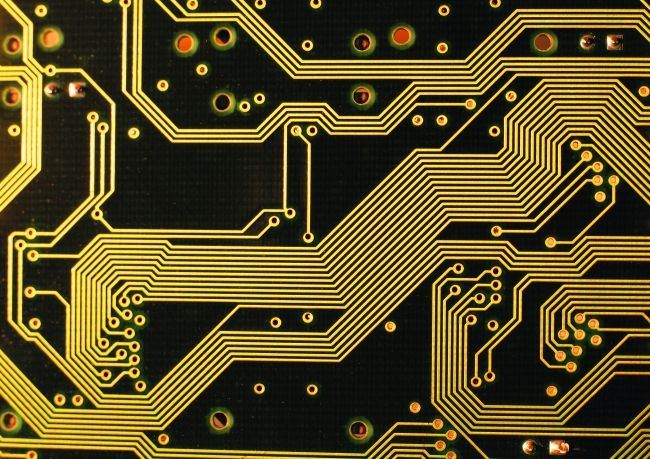
- Wiring should be properly done without interference and cross. For example, input/output, AC / DC, strong / weak signal, high frequency / low frequency, high pressure / low voltage, etc., the wiring direction should be like linear or separated without blending to each other for the purpose of avoiding mutual interference. The best wiring is like straight line, but it’s difficult to achieve. For DC, small signal, low voltage PCB design can lower the requirement properly. Besides, The edges of the input end and output end should be prevented from being parallelly adjacent in order to avoid reflection interference. If necessary, ground isolation should be added, two adjacent layers of wiring should be perpendicular to each other, parallel is prone to parasitic coupling.
- Select a good grounding point: normally it requires a mutual point, digital and analog ground are connected in the power input capacitor.
- Reasonable layout of the power supply filter / decoupling capacitors: the layout of these capacitors should be as close as possible to the electronic components because there will be no effect if it’s too far away.

- Wires are better to be wide; high pressure and high frequency wire should be pliable, sharp chamfer is not allowed, the corner should not be used at right angle, normally 135 degree angle instead. Ground wire should be as wide as possible, it’s best to use a large area of coating copper, which has a considerable improvement to the grounding points. In addition, over-line holes are not allowed in the design, and reduce the density of parallel lines.
- Widen the power wire and grounding wire as far as possible, but the latter should be wider than the former, in short, their relationship is: grounding wire > power wire> signal wire.
- Digital circuit and analog circuit share a common grounding point, there are many PCB is no longer a single functional circuit (digital or analog circuit), instead, they comprise the mix of digital circuit and analog circuit. Thus, consider the mutual interference issue when wiring, especially the noise interference from the ground wire.
