Currency
Toggle Nav

The Unseen Dance of PCB Assembly Beyond the Blueprint
April 23, 2025
Ever held a sleek gadget, a powerful sensor, or maybe even a compact LoRa module, and marveled at its capabilities? We often admire the final product, the elegant design, the seamless function. But beneath that polished surface lies a hidden world of incredible precision, complex choreography, and technological artistry – the world of PCB Assembly (PCBA). It's a story rarely told, yet it’s the very process that breathes life into the electronic devices shaping our future, especially in the rapidly expanding realm of IoT and LoRa technology. Let's pull back the curtain.
The Spark of Creation: From Design to Data
The journey begins not with solder, but with data. A designer meticulously lays out a circuit, placing components virtually, routing connections – creating the blueprint. This digital design package (Gerber files, Bill of Materials, Placement data) is the script for the assembly performance. It dictates exactly where every resistor, capacitor, integrated circuit, and crucially, sensitive components like LoRa transceivers, must go. The accuracy here is paramount; a misplaced component, even by a fraction of a millimeter, can spell disaster for the final product's functionality, particularly for sensitive RF circuits used in LoRaWAN devices.
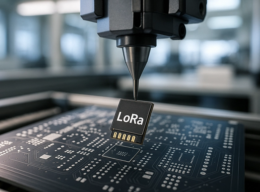
PCB assembly
Act I: The Stencil and the Paste
The first physical step is applying solder paste. Think of it like screen printing, but with metallic glue. A thin stainless steel stencil, precisely laser-cut with openings matching the component pads on the bare PCB, is laid over the board. Solder paste – a mixture of tiny solder spheres and flux – is squeegeed across the stencil, leaving perfect deposits only where components will sit. This stage sets the foundation; the quality of the paste deposition directly impacts the strength and reliability of the solder joints, which is critical for devices, like LoRa nodes, often deployed in challenging environments.
Act II: The Pick-and-Place Ballet
Now comes the high-speed ballet: the Pick-and-Place (PnP) machine. Fed by reels of components, robotic arms equipped with vacuum nozzles pick up individual parts – from minuscule resistors to complex ICs, including the essential LoRa modules – and place them onto their corresponding pads on the PCB with breathtaking speed and accuracy. Modern PnP machines can place tens of thousands of components per hour. Watching this process is mesmerizing – a blur of motion guided by sophisticated computer vision systems ensuring every piece lands exactly right. This precision is non-negotiable for densely packed boards common in modern LoRa applications.
Act III: The Trial by Fire (Reflow Soldering)
With components delicately perched on the solder paste, the board embarks on a carefully controlled journey through a reflow oven. This isn't just about heat; it's about a precise thermal profile. The board slowly heats up (preheat), stabilizes at a specific temperature (soak), spikes to melt the solder (reflow), and then carefully cools down. This process transforms the dull grey paste into shiny, strong solder joints, permanently bonding the components to the board. An incorrect profile can damage sensitive parts or create weak joints, compromising the long-term reliability of any electronic device, let alone a critical LoRaWAN gateway.
Intermission: Inspection and Quality Control
Perfection is the goal. After reflow, boards often undergo Automated Optical Inspection (AOI). Cameras scan the board, comparing it against the design data to catch placement errors, solder bridges, or insufficient solder. For hidden joints, like those under Ball Grid Arrays (BGAs) sometimes found in advanced LoRa system-on-chips, X-ray inspection might be used. This rigorous checking ensures that the intricate assembly for LoRa communication pathways is flawless.
Act IV: The Human Touch and Final Testing
While automation handles much of the surface-mount process, some components (Through-Hole Technology) might still require manual insertion and soldering. Skilled technicians play a crucial role here. Finally, the assembled board faces its ultimate test: functional testing. Does it power up? Does it communicate? For a LoRa device, this means checking if the radio transmits and receives correctly, ensuring the core LoRa functionality meets specifications.
The Encore: Enabling Innovation
This intricate dance – from digital file to fully functional circuit board – is the unsung hero behind countless technological advancements. Services that streamline this process, like the PCB assembly sponsorships sometimes offered, are vital for innovators, especially those working on cutting-edge LoRa projects. They lower the barrier to entry, allowing brilliant ideas involving LoRa technology to move from concept to reality faster and more affordably. The story of PCB assembly isn't just about machines and solder; it's about enabling the next wave of connected devices, powered by technologies like LoRa.