Six Steps to Fulfill the Whole PCB Manufacturing Process
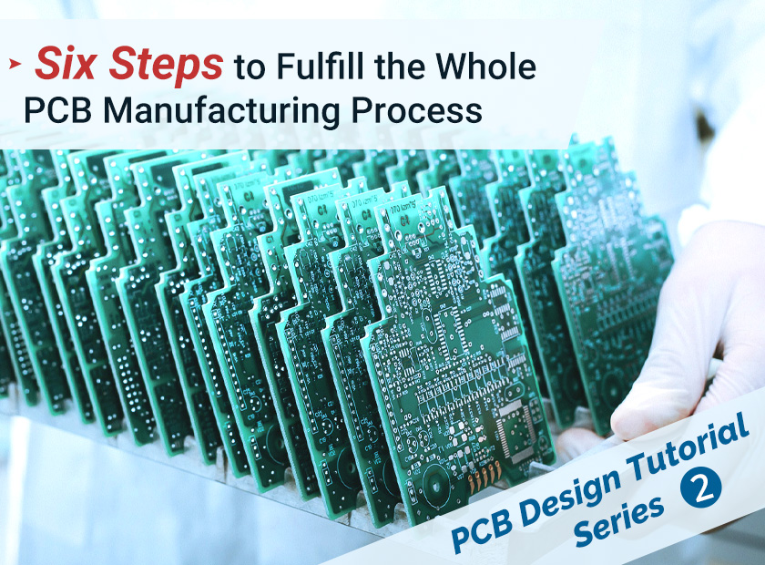
In the previous article, we’ve discussed about details in designing a PCB. Then comes the second and meanwhile the most tricky part - PCB manufacturing. Printed circuit boards (PCBs) are the basis of most modern electronic devices. They have wiring and pads connecting individual points together. Generally speaking, it takes 6 steps to make a PCB. Now, we will introduce them one by one through pictures.
PCB CAD Files
The first step of PCB manufacturing is to organize and check PCB layout. Each CAD software has its own unique file format. CAD files should be converted into a unified format - extended Gerber RS-274X or Gerber X2. Then PCB layout should be checked whether it conforms to the manufacturing standards or bears any defects. The PCB layout can be printed on paper with a laser printer and then transferred to a copper clad plate. In the printing process, the printer is prone to lacking ink or creating breakpoints, so it is necessary to manually replenish ink with an oily pen.
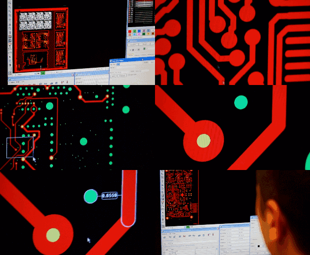
Plate-making
Clean the copper plate. Dust may cause a short circuit or a broken circuit. PCBs with different layers require different amounts of copper clad plates and copper films. Take an 8-layer PCB for example. It is made of 3 copper clad plates plus 2 copper films, which are then bonded together with prepreg. The production sequence starts with the middle board (Layer 4 and Layer 5 circuits) which are stacked together layer by layer. The 4-layer PCB is similarly made, including a core plate and two copper films.
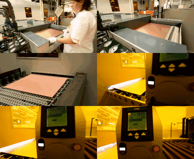
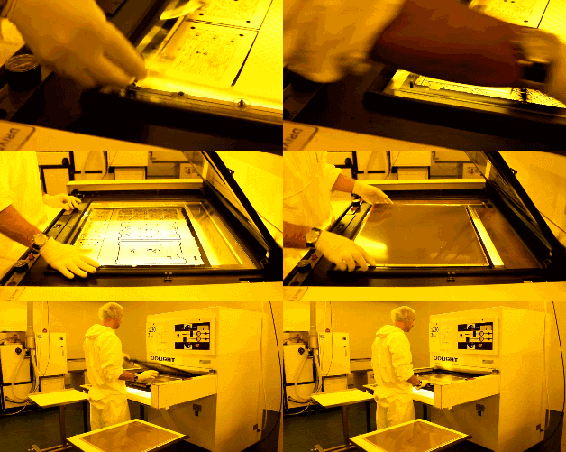
After cleaning the copper-clad plate, the surface of which will be covered with a photosensitive film. This film solidifies when contacting with light and forms a protective film on the copper foil. Insert two layers of PCB cabling film and a double layer of copper coated plate into the upper PCB cabling film to ensure accurate stacking of the upper and lower PCB cabling films.
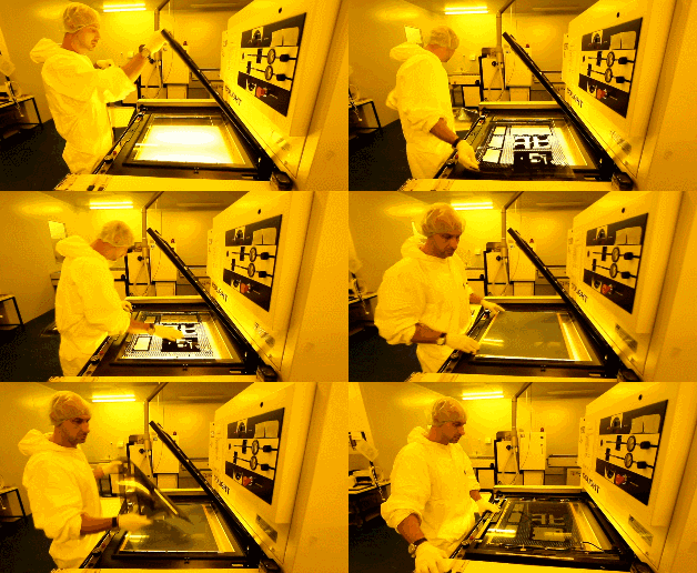
Irradiate the photosensitive film on the copper foil with a UV lamp. The transparent film cures under light, and there is still no cured photosensitive film. The copper foil covered under the curing film is required for PCB layout, which is equivalent to the role of laser printer ink for manual PCBs. In addition, the copper foil covered by the black film will be corroded, and the cured transparent film will be preserved.

Wash the uncured film with lye and the cured film will cover the copper foil circuit. Then use a strong base, such as NaOH, to etch off the unwanted copper foil. Tear off the cured photosensitive film to expose part of the copper foil needed for the PCB layout.
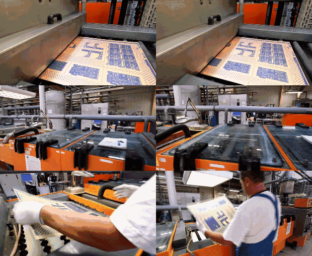
Board-proofing and Check
Align holes in the core plate for lamination with other materials. Once the core board is laminated with other laminates, it cannot be modified. That’s why PCB inspection is necessary and very important. At this stage, the first two layers of PCB board have been made successfully.
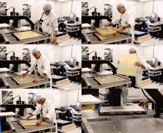
Lamination
The lamination requires a new material, prepreg, which acts as the adhesive between the core plate and between the core plate and the outer copper foil. The lower copper foil and two layers of prepreg have been fixed by the trace hole and the lower iron plate, and then place the finished core plate in the trace hole. Finally, cover a layer of copper foil and a layer of pressure-bearing aluminum plate on the core plate.

Hole-drilling
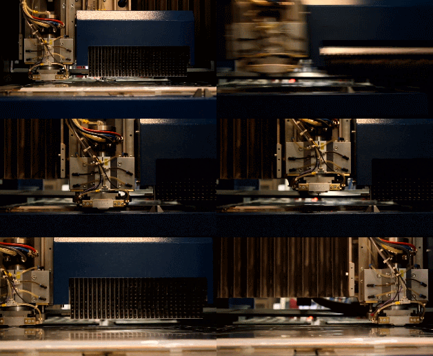
Then how to connect four layers of copper foil in PCB? Firstly, the PCB is perforated and then the hole walls are metallized to conduct electricity. Lay a layer of aluminum plate on the punching machine and place the PCB on top. Finally, cover the topmost PCB with a layer of aluminum plate. The upper and lower aluminum plates are used to prevent the copper foil on the PCB from tearing when drilling.
Since almost all PCB designs use perforations to connect different layers of wires, a 25-micron copper film needs to be laid on the hole wall. The thickness of the copper film is decided by galvanization. The pore wall consists of non-conductive epoxy resin and glass fiber board. So the first step is to deposit a layer of conductive material on the pore wall, and chemical deposition forms a 1 micron copper film on the entire PCB surface.
PCB Outer Layer processing
Transfer the PCB outer layer to the copper foil. The process is similar to the transfer process of the previous PCB core board. The PCB layout is transferred to the copper foil by using photocopying film and photosensitive film.
The PCB is covered by a cured photosensitive film as a circuit to clean the uncured film. After etching of the exposed copper foil, the PCB layout circuit is protected by a cured film. The transfer of the outer PCB layout adopts the normal method. The non-circuit area is covered by a cured photosensitive film on the PCB. After cleaning the uncured film, electroplating is performed. Where there is a film, it cannot be electroplated, and where there is no film, it should be plated with copper before tin. After the film is removed, alkaline etching is performed and finally the tin is removed. Finally, the tin-plating layer on the copper foil of PCB layout should be removed and cleaned with tin-stripping liquid.
After all these complex processes, a 4-layer PCB is completed at last. This whole process involves many sophisticated details like chemical treatment and cleaning that need to be controlled by computers to ensure accuracy.

