Optimizing PCB Design with Advanced DFT Strategies

Optimizing PCB Design with Advanced DFT Strategies
Implementing a design for test (DFT) in PCB (printed circuit board) design is crucial in ensuring that the board can be tested effectively and efficiently. Testing (DFT) is an integral step in the PCB design process with the rise of thinner boards, more powerful components, and denser layouts. Today's manufactured PCBs are becoming more complex, requiring intense and precise testing to guarantee they work as intended. At Elecrow, we used advanced technology for the DFT of your circuit board and the PCBA process.
Design engineers need to ensure that the PCB testing process is efficient while minimizing the testing cost. To achieve this goal, we have shown you how design engineers consider the feasibility of testing before the design process begins. DFT is a design methodology that enhances the testing efficiency of a PCBA by considering the testing requirements. This article will check the design for test integration in PCBA, including the methods, benefits, and common challenges while implementing the design for test in your circuit.
 What is Design for Testability (DFT)?
For starters, design for testing is a set of design techniques and methodologies used in electronic design, mostly in PCB and IC design.
Design for test ensures that a product can be easily and thoroughly tested for defects. The goal of design for testing is to make testing more efficient and reliable while also achieving less expensive results. This, in turn, helps to improve the product quality and reduce the extra time needed for troubleshooting.
One key objective of the design for test is to simplify the testing process so that it can be performed quickly with minimal effort. Design for tests ensures comprehensive testing to detect as many faults as possible within a short period of time, reducing the cost of PCBA manufacturing.
 Parameters to Include in Design for Test
DFT involves many parameters and considerations to ensure that the product works flawlessly. Therefore, including the test parameters while designing PCB can significantly improve the tests, reduce costs, and enhance the product's reliability. Let's look at some of the parameters below:
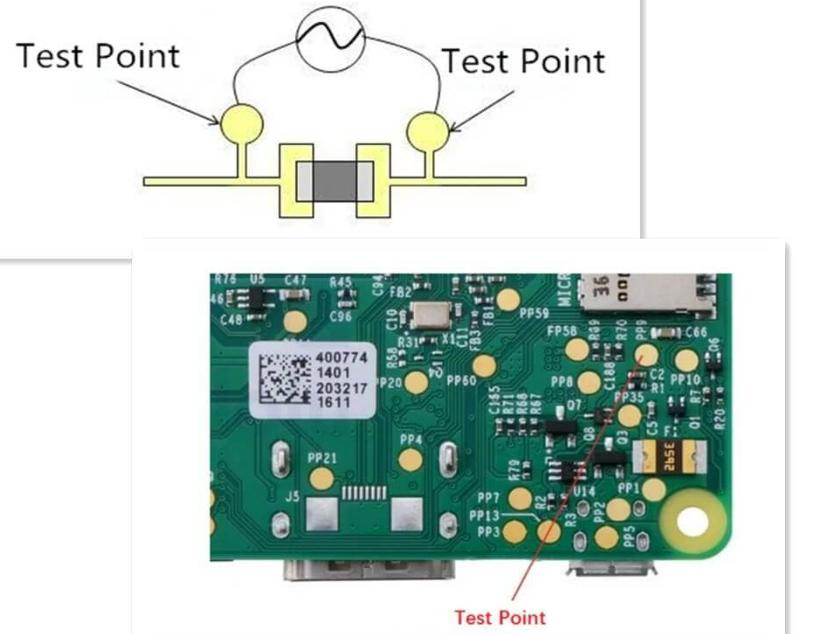
- Test Points: They are placed on the specific locations on the PCB that are accessible for testing. The position of the test point is designed based on the number of components that it can cover. Some signal integrity issues can occur. But this can simply be resolved by arranging accurate power and ground test points.
- Test Traces: The test points can be directly placed on the traces. Test traces reduce the reliance on physical probing, which can also be very challenging and imprecise. Test traces are mostly used for sensitive PCBs, where the Automated test equipment (ATE) can easily interface with test traces, allowing for more efficient and accurate testing processes.
- Headers: These are the test points connected to the vias and/or traces. They are used to connect the oscilloscopes or measure the voltages across them. Headers guarantee consistent and repeatable connections, which is essential for reliable testing.
- LEDs: LEDs are included on the PCB specifically for the testing purpose. It can determine whether the power is switched on or off. It also offers instant visual confirmation of data transfer or any error conditions.
 Benefits of Design for Test
DFT is a major factor in the electronic design and manufacturing industry today. Thus, let’s look at why all the circuit boards must pass the DFT check and what are the major benefits of DFT in the below points:
Early Fault Detection
DFT helps designers and engineers identify defects and errors while designing circuit boards. This helps troubleshoot and prevent further problems that could cause further issues in circuit board assembly.
Improves Product Quality
Through DFT, designers and engineers can easily identify and fix hidden errors. Thus, it helps to maintain the quality of the products. Through proper testing, designers can better understand the behavior and performance of the circuit board. This ultimately improves the product quality.
Reduce Cost
Testing helps the designer identify issues and fix them in an earlier development stage. This helps reduce the risk of production failures and errors. Industry examinations show that testing can reduce the cost up to 50 percent, 60% of rework flow, and 15% of defect rate.
Scalability and Flexibility
DFT allows the development of a flexible and scalable testing framework that can be adapted to various technologies and products.
Faster Time to Market
Early fault detection and debugging lead to faster design validation with shorter development cycles. This speeds up testing time and quicker fault resolution, speeding up the production process.
 Methods of Integrating Design for Test
Integration of DFT in PCB design is the essential step in the PCBA process. Special methods and considerations are required while integrating DFT in the PCB domain. We will see some of the common methods of implementing DFT in PCB design below:
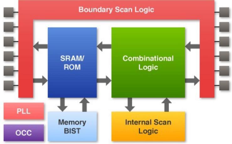
Boundary Scan
The testing methods test each component within a PCB. In this method, the boundary scan cell is added to a PCB design. It allows the testing of signals. This method can help troubleshoot issues like open or short circuits, incorrect pin assignments, and more, which makes it easier to test any complex boards.

Built-In Self-test (BIST)

This method allows a device to test itself, reducing the need for external testing equipment. It helps to reduce costs and test time. BIST can be built into the device or added through external hardware.
BIST features let the PCB test itself, finding faults inside without needing extra equipment. It can also run diagnostics during normal use, providing constant monitoring and fault detection.
Fault Isolation Design
DFT aims to cover all possible faults and make diagnosis easy. It identifies faults and provides clear and proper information about their presence and nature. This helps in quick debugging. Designing for fault isolation helps quickly find and separate faults using test points, fault identification circuits, or fault segregation techniques.
Power and Ground Isolation
Isolating power and ground segments allows for independent testing of different PCB sections. It improves fault isolation and detection. It helps to reduce the noise. Reducing noise and interference during testing ensures more accurate results.

Test Points
When designing PCB hardware, strategically placing test points is key to easy access during testing. This makes testing more efficient and helps quickly identify issues, saving time and effort.

 Common Challenges While Implementing Design for Test
The major challenges in implementing the design for test include:
Space Constraints
In the 5G advanced era, small PCBs have taken a separate place in modern electronics. With the rise of miniaturization, circuit board testing is one of the major challenges today. The compact design requires careful consideration and some advanced solutions for effective circuit board testing.
Performance Overheads
The addition of DFT circuitry can include power consumption that could affect the performance of the final product. Furthermore, these test-related circuits could slow down the overall operational speed of the devices.
High-Density Packing
If you see any high-quality PCBA, it is highly densely packed. This helps accommodate numerous components in the tightly packed areas. To include DFT in tightly packed designs, careful planning is needed to place test access points in the right spots without interfering with the important parts.
Precision and Signal Integrity
A high-quality PCB has proper signal integrity, mainly with high-speed data transfer. Implementing the features of DFT without compromising signal quality is a major challenge in the PCBA domain. The addition of more test points in the circuit board can lead to an impedance mismatch, causing signal reflections.
Advanced and Complex Technologies
The fast-paced technological changes constantly challenge PCB designers to keep up with the newest DFT methods and tools. Dealing with this complexity requires ongoing learning and adjusting design practices to fit new trends.
 Conclusions
Thus, integrating design for testing into your circuit board during the PCBA process ensures effective testing and high-quality products. The importance of design for test has increased with the rise and advancement of miniaturized PCBs. Engineers and designers could benefit significantly by integrating DFT during the design process.
At Elecrow, we provide advanced DFT strategies that streamline the testing processes, help reduce costs, and shorten the time to market. We also provide free functional PCBA testing for our customers. Thus, grab this opportunity today and check out the one-stop electronic solutions at Elecrow.
