Currency
Toggle Nav

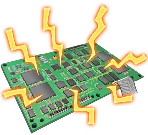
How to improve the anti-electromagnetic interference when developing electronic products with processors?
November 01, 2017
1.Anti-electromagnetic interference issue should be more careful with the following systems
1)The system that the microcontroller clock frequency is particularly high and the bus cycle is particularly fast.
2)The system contains high-power and high current drive circuit, such as the relay with a spark, high current switch and so on.
3)The system with a weak analog signal circuit and high-precision A / D converter circuit.
2. Measures to improve the anti-electromagnetic interference of system
1)Choose the low-frequency micro-controllers.
The use of low external clock frequency micro-controllers can effectively reduce the noise and improve the system's anti-jamming capability. The square wave and sine wave at the same frequency, the high-frequency components of the square wave are much more than the sine wave.
2)Reduce the distortion in the signal transmission.
Micro-controllers are manufactured using high-speed CMOS technology. The static input current at the end of signal input is about 1mA, the input capacitor is 10PF or so, the input impedance is very high, the output end of high-speed CMOS circuit has a considerable load capacity, that is a considerable output value. An output end through a very long line leads to an input end with a very high impedance, the reflection problem is very serious. It will cause signal distortion, increase system noise. When Tpd> Tr, it becomes a transmission line problem, in this case, you must consider the signal reflection, impedance matching issues.
The delay time of the signal on the printed circuit board is related to the characteristic impedance of the lead which means the dielectric constant of the printed circuit board material. It can be roughly assumed that the transmission speed of the signal in the printed circuit board lead is about 1/3 to 1/2 of the speed of light. The Tr (standard delay time) of the commonly used logical telephone elements in the system constituted by the micro-controllers is between 3 and 18ns.
In the printed circuit board, when the signal goes through a 7W resistor and a 25cm long lead, the line delay time is between 4 ~ 20ns. In other words, the shorter the signal lead on the printed line is, the better the signal will be(25cm is the max. length). And the number of vias should be as little as possible, preferably no more than two.
Use the following conclusion to summarize a rule for printed circuit board design:
The signal is transmitted on the printed board and its delay time should not be greater than the nominal delay time of the device used.
3)Reduce the cross interference between signal lines.
4)Reduce the noise from power.
When the power supplies energy to the system, it also brings noise to the power it supplies. In the circuit, the reset line, junction line and the other control lines of micro-controller are the most sensitive parts to the interference of noise.
5)Be careful with the high-frequency characteristic of electronics parts and the printed board.
6)Components placement should be in a reasonable distribution.
EMI must be taken into consideration for the placement of components on the printed circuit board, one of the rules for avoiding this issue is to make the lead line between components as short as possible. In the layout, it’s necessary to properly separate the three parts: Analog signal part, high-speed digital circuit part and noise source part(like relays, large current switches), doing so can ensure the minimum signal coupling between each other.
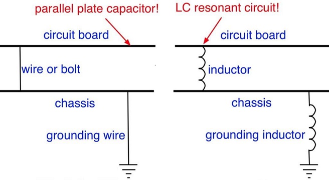
7)Properly handle the grounding line.
On the printed circuit board, power line and grounding line are the most important parts. To overcome the EMI, grounding is the main method.
For the double-sided board, the layout of grounding line is particularly rigorous. Using the method of single-point grounding, power and ground are connected to the printed board from both ends of the power supply, and both the power and the ground have a contact. On the print circuit board, there must be multiple return grounding lines and all of which will be gathered back to the contact of power, this is the so-called single point grounding.
Circuits that are very sensitive to noise and interference or circuits with severe high-frequency noise should be shielded with metal shields.
 8)Make the best of decoupling capacitors.
A good high-frequency decoupling capacitor can eliminate high-frequency elements up to 1GHZ. Ceramic chip capacitors or multilayer ceramic capacitors have a good high-frequency characteristic. When designing a printed circuit board, there must be a decoupling capacitor between the power and grounding of each integrated circuit.
Decoupling capacitors have two effects: on the one hand it is the storage capacitor of the integrated circuit aiming to provide and absorb the charge and discharge energy generated at the moment of opening and closing the circuit; on the other hand, it can bypass the high-frequency noise of the device. The typical decoupling capacitor in the digital circuit is 0.1uf with a 5nH distributed inductance, its parallel resonant frequency is about 7MHz, which means it has a better decoupling effect on the noise below 10MHz and almost no effect on the noise above 40MHz.
3.More tips to reduce noise and EMI
1) Low-speed chip is more recommended to use compared to the high-speed chip which is used in the key points.
2) Provide damping in some form for the relay as far as possible.
3) Use the lowest frequency clock that meets the system requirements.
4) Circle up the clock area with the grounding line, the clock line should be as short as possible.
5) A decoupling capacitor is needed for each integrated circuit, and a small high-frequency bypass capacitor should be added to the side of each electrolytic capacitor.
6) Don’t form any signal loop, if unavoidable, make the loop area as small as possible.
7) Component pins need be as short as possible and decoupling capacitor pins should be as short as possible.
8) Analog voltage input line, the reference voltage side should be away from the digital circuit signal line as far as possible, especially the clock.
9) Important lines should be as thick as possible and add protection on both sides. The high-speed line must be short and straight.
10) Noise-sensitive lines should not be parallel to the high-current, high-speed switching lines.
The EMI issue is considered as a big headache for many electronic makers when doing PCB layout because it’s a key of the high-quality printed circuit boards and involves a plenty of knowledge and experiences of electronics and hardware structure. With the constant research in hardware innovation and development, Elecrow provides solutions and technical support for makers to help make their ideas come true, so you are welcome to talk with our experienced engineers for any question.
8)Make the best of decoupling capacitors.
A good high-frequency decoupling capacitor can eliminate high-frequency elements up to 1GHZ. Ceramic chip capacitors or multilayer ceramic capacitors have a good high-frequency characteristic. When designing a printed circuit board, there must be a decoupling capacitor between the power and grounding of each integrated circuit.
Decoupling capacitors have two effects: on the one hand it is the storage capacitor of the integrated circuit aiming to provide and absorb the charge and discharge energy generated at the moment of opening and closing the circuit; on the other hand, it can bypass the high-frequency noise of the device. The typical decoupling capacitor in the digital circuit is 0.1uf with a 5nH distributed inductance, its parallel resonant frequency is about 7MHz, which means it has a better decoupling effect on the noise below 10MHz and almost no effect on the noise above 40MHz.
3.More tips to reduce noise and EMI
1) Low-speed chip is more recommended to use compared to the high-speed chip which is used in the key points.
2) Provide damping in some form for the relay as far as possible.
3) Use the lowest frequency clock that meets the system requirements.
4) Circle up the clock area with the grounding line, the clock line should be as short as possible.
5) A decoupling capacitor is needed for each integrated circuit, and a small high-frequency bypass capacitor should be added to the side of each electrolytic capacitor.
6) Don’t form any signal loop, if unavoidable, make the loop area as small as possible.
7) Component pins need be as short as possible and decoupling capacitor pins should be as short as possible.
8) Analog voltage input line, the reference voltage side should be away from the digital circuit signal line as far as possible, especially the clock.
9) Important lines should be as thick as possible and add protection on both sides. The high-speed line must be short and straight.
10) Noise-sensitive lines should not be parallel to the high-current, high-speed switching lines.
The EMI issue is considered as a big headache for many electronic makers when doing PCB layout because it’s a key of the high-quality printed circuit boards and involves a plenty of knowledge and experiences of electronics and hardware structure. With the constant research in hardware innovation and development, Elecrow provides solutions and technical support for makers to help make their ideas come true, so you are welcome to talk with our experienced engineers for any question.