How To Create Unique PCB Design?
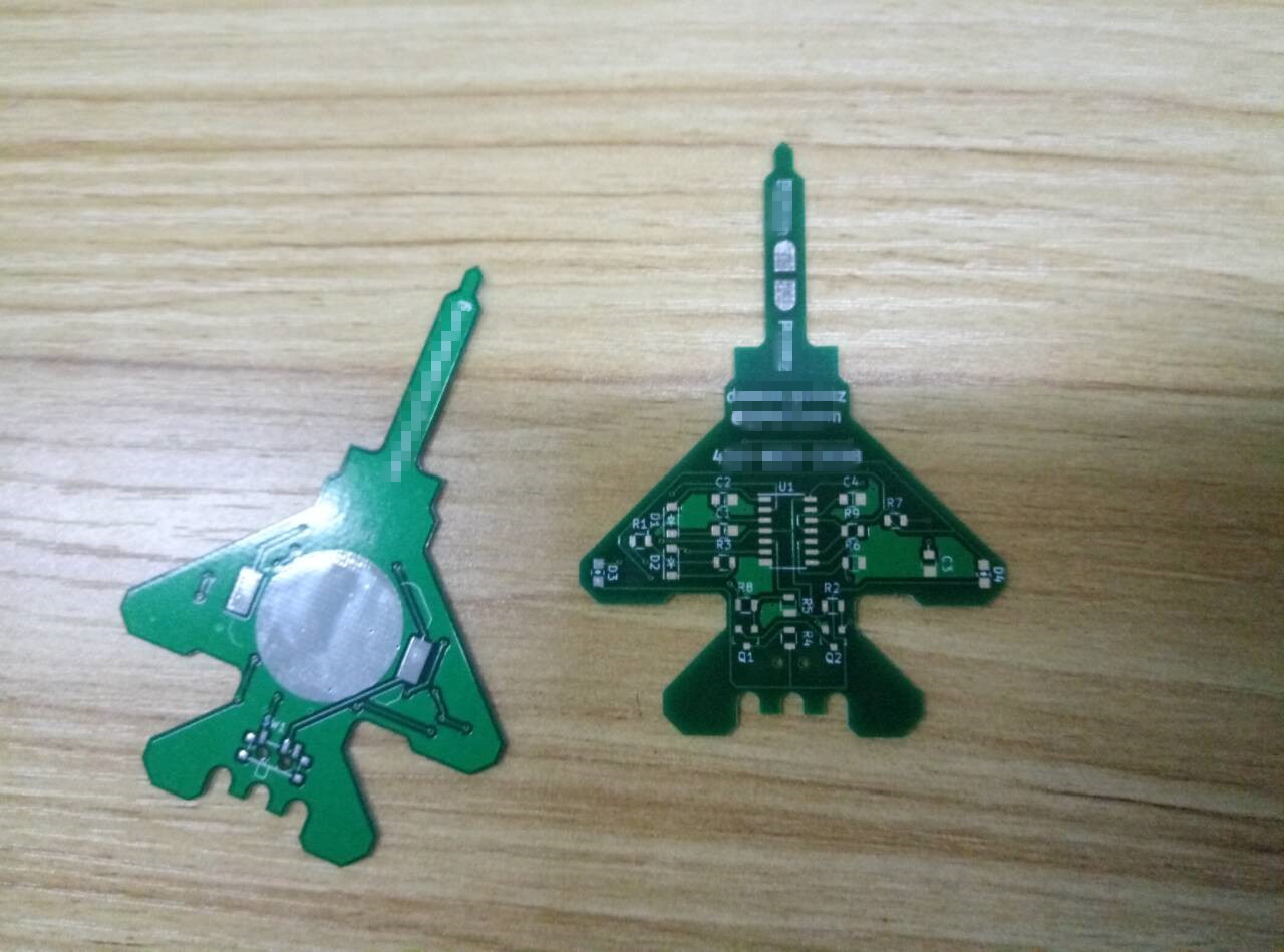
PCB world is really magical and broad for makers to create various useful projects. As we know, it is a board that has lines and pads to connect various points together and sort of like a layer cake for its laminated substrate,copper,soldermask and silkscreen together with heat and adhesive. Nowadays plenty of makers are paying more attention to the design of PCB. They would like to make PCB this dull thing filled with innovation and creativity to satisfy people's fancy demand. So it comes to today's topic: How To Create Circuit Boards For Unique PCB Design? Here are two main methods for unique pcb design: Special silkscreen layer arts& Shapes custom. Shapes custom The following pictures are shapes custom-made air plane pcb ( made by elecrow creative customer) and christmas tree pcbs. These pcbs are cool and pretty-looking meanwhile you can apply them into certain projects. Only if you get fantastic ideas and design inspiration for applied components, you could also design one unique shape custom-made pcb. 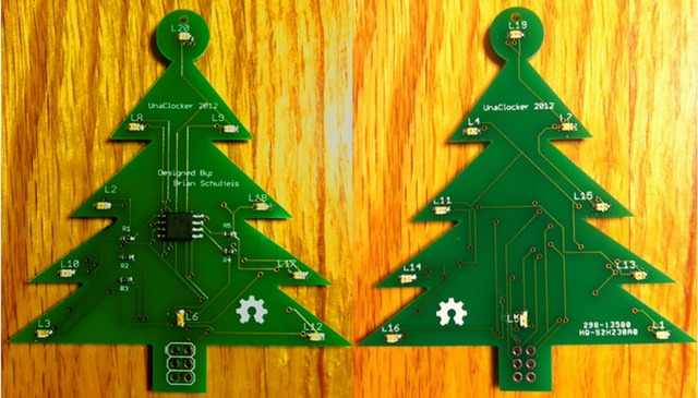
 Special silkscreen layer arts
You could see that following picture seems like people sketch but it is not made by drawing definately.Yeah it is the magic of silkscreen layer art. 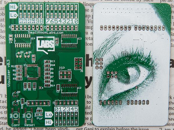
During the process of creating silkscreen layer, I selected several details you need to notice. First of all, you are supposed to make sure that all components, installation holes and positioning holes have counterpart of silk printed labels so as to make it convenient for the installation of the board. Secondly, the identifier of the device on the PCB must be consistent with the identity symbol in the BOM list. Thirdly, when you draw dashed lines, you ought to paste and copy little by little to make dashed components and then you could cluster these components to transfer them into gentle lines. Last but not the least, when you import the schematic diagram to netlist, you had better pay attention to the “Designator” installation to adjust the size of your design in case the design comes out of shape. 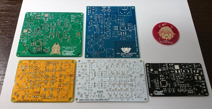 Follows I sincerely shared some selected helpful and corresponding reference for your making *^-^* PCB Design – Making Your PCB as Small as Possible 6 Tips to Ensure Great PCB Designs how to design the perfect pcb Tips for Designing PCBs Designing pcb Quick and Simple PCB designing
Circuit Skills: Circuit Board Etching
Our PCB service also plays an essential and active role for many makers around the world, if you like and wonder, welcome to know more and have a try ^ω^
