Currency
Common PCB Assembly process defects and cause analysis
March 22, 2022

Common PCB Assembly process defects and cause analysis
Learn these PCBA process defects and get twice the result with half the effort in the design phase
Many engineers in the R & D verification stage, in order to save time, will look for the PCBA factory to make the sample, but due to the different level of factory technology, some engineers have found a short circuit or open circuit after got the sample, Unable to test normally and can't find the problem at the moment, It's not sure whether it's a factory problem or a design issue, Therefore, we collected several common process defects in PCBA processing to help you to avoid detours.
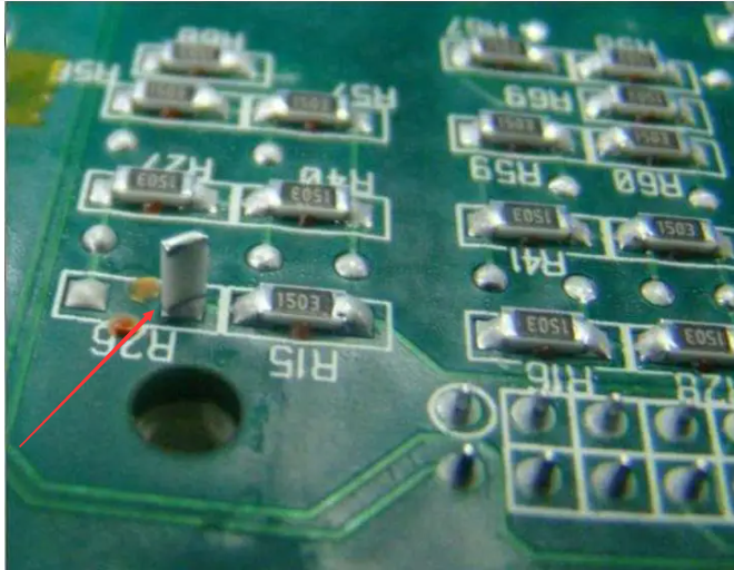
Defect 1: the phenomenon of "erecting stele" (i.e. chip components "erecting") [defect explanation] it is usually due to the unbalanced wetting force at both ends of the component during reflow soldering, resulting in unbalanced torque at both ends of the component, resulting in "erecting stele".

Factor A: unreasonable pad design and layout
① One of the pads on both sides of the element is connected with the ground wire, or the area of one side pad is too large, and the heat capacity at both ends of the pad is not uniform;
② The temperature difference on the PCB surface is too large, which leads to uneven heat absorption on both sides of the component pad;
③ There will be an uneven temperature at both ends of the pad of small chip components around large devices QFP, BGA, and radiator.
Solution: engineers adjust pad design and layout
Factor B: solder paste and solder paste printing problems
① If the activity of solder paste is not high or the solderability of components is poor, the surface tension will be different after the solder paste melts, which will cause the imbalance of pad wetting force.
② The solder paste printing quantity of the two pads is uneven. One side of the solder paste is thick and the tension is large, while the other side is thin and the tension is small. As a result, one end of the component is pulled to one side to form an empty solder joint, and the other end is pulled up to form a monument.
Solution: the factory needs to select solder paste with high activity to improve the printing parameters of solder paste, especially the window size of steel mesh
Factor C: uneven stress in z-axis direction of chip displacement. This situation will lead to an uneven immersion depth of components in solder paste and an unbalanced wetting force on both sides due to time differences during melting. If the chip displacement of components will directly lead to stele erection.
Solution: the factory needs to adjust the process parameters of the placement machine
Factor D: the furnace temperature curve is not correct. if the reflow soldering furnace body is too short and the temperature zone is too small, it will cause the working curve of PCB heating is not correct, so that the moisture difference on the board surface is too large, resulting in the imbalance of wetting force.
Solution: the factory needs to adjust the appropriate temperature curve according to each different product.
Defect 2: "tin bead" phenomenon
Factor A: the temperature curve is not correct. The reflow curve can be divided into four sections: preheating, heat preservation, reflow, and cooling. The purpose of preheating and heat preservation is to make the surface temperature of PCB rise to 150 ℃ within 60-90 s and heat preservation for about 90 s. This can not only reduce the thermal impact of PCB and components but also ensure that the solvent of solder paste can be partially volatilized, so as to avoid splashing caused by too much solvent during reflow soldering, which will cause solder paste to rush out of the pad and form solder beads.
Solution: the factory should pay attention to the heating rate and take appropriate preheating to make the solvent volatilize fully
① The metal content in solder paste is usually (90 ± 0.5)%, too low metal content will lead to too much flux composition, so too much flux will cause flying bead because it is not easy to volatilize in preheating stage;
② The increase of water vapor and oxygen content in solder paste can also cause flying bead. Because solder paste is usually refrigerated, if it is not thawed and stirred evenly when it is taken out from the refrigerator, it will cause water vapor to enter; in addition, the lid of solder paste bottle should be tightly closed after each use, if it is not closed in time, it will also cause water vapor to enter;
③ After the solder paste printed on the steel screen is completed, the remaining part should be treated separately. If it is put back into the original bottle, the solder paste in the bottle will deteriorate and tin beads will be produced;
Solution: the factory is required to select high-quality solder paste and pay attention to the storage and use requirements of solder paste
There are other factors
① The printing is too thick, and the excess solder paste overflows after the component is pressed down;
② The mounting pressure is too high, the solder paste collapses to the ink;
③ The shape of the pad opening is not good, and the solder bead prevention treatment is not done;
④ Solder paste activity is not good, dry too fast, or there are too many small particles of tin powder;
⑤ Printing offset, so that part of the solder paste stick to the PCB; 6. Too fast scraper speed, resulting in poor edge collapse, lead to solder ball after reflow.
Defect 3: "bridging" phenomenon
Factor A: the quality problem of solder paste
① The metal content in solder paste is high, especially if the printing time is too long, it is easy to increase the metal content, leading to IC pin bridging;
② The viscosity of solder paste is low, and it flows out of the pad after preheating;
③ The drop of solder paste tower is poor, and it flows out of the pad after preheating;
Solution: the factory needs to adjust the proportion of solder paste or use a good quality solder paste
Factor B: printing system
① The printing press has poor repetition accuracy and uneven alignment (inaccurate alignment of steel mesh and PCB), which leads to solder paste printing outside the pad, especially the fine pitch QFP pad;
② The inaccuracy of the size and thickness of steel mesh window and the uneven Sn Pb alloy coating of PCB pad lead to more solder paste;
Solution: the printing press needs to be adjusted in the factory to improve the coating layer of PCB pad;
Factor C: too much-sticking pressure and full flow of solder paste after being pressed are the common reasons in production. In addition, insufficient accuracy of the chip will cause the components to shift and IC pins to deform;
Factor D: reflow furnace temperature rising speed is too fast, solvent in solder paste is too late to volatilize
Solution: the factory needs to adjust the z-axis height of the placement machine and the heating speed of the reflow soldering furnace.
Defect 4: "wicking" phenomenon, also known as a material suction phenomenon and core pulling phenomenon, is more common in gas phase reflow soldering. The solder separated from the pad and went up between the pin and the chip body, which led to serious false soldering. Generally, due to the high thermal conductivity and rapid temperature rise of the pins, the solder preferentially moistens the pins, and the wetting force between the solder and the pins is much greater than that between the solder and the pad, and the up warping of the pins will aggravate the phenomenon of wicking.
Solution: the factory needs to preheat the SMA (surface mount assembly) fully before welding in the furnace. It should carefully test and ensure the solderability of PCB pad. The coplanarity of components can not be ignored. The components with poor coplanarity should not be used in production. Note: in the infrared reflow soldering, the organic flux in PCB substrate and solder is a good absorbing medium for infrared rays, while the pin can partially reflect infrared rays. Therefore, the wetting force between solder and pad will be greater than that between solder and pin, so the solder will not rise along with the pin, so the probability of the wicking phenomenon is much smaller.


