Currency
6 elements you need to check in the late PCB design
November 10, 2017

When a PCB layout and routing is completed and both the connectivity and spacing are inspected without faults, does it mean the PCB design is succeeded and finished? Of course no. A final inspection is often ignored or neglected by some new engineers, this is likely to result in some bugs or problems in prototyping or even re-prototyping, such as the sockets getting too close, or loop signal and so on. Therefore, a final inspection is a must-do thing of PCB layout.
A good final inspection process involves lots of specific steps, here listed some steps that I found quite important but easy to be ignored.
1.Footprint
1). Pads spacing. For the new components, it’s necessary to draw the footprint by yourself so as to make sure a proper spacing, because the pad spacing has an immediate effect on the components soldering.
2). Size of vias. For the plug-in components, the vias should keep some extra space for the assembly, the proper space is normally no less than 0.2mm.
3). Silkscreen. The outline silkscreen of components should be bigger than the actual size, this is to ensure the components could be assembled smoothly.
2. PCB Layout
1). IC should not be close to the edge of printed circuit board.
2). The components for the same module circuit function should be closely placed. For example, the decoupling capacitor should be close to the IC’s power foot, and the components make up the same functional circuit should be given priority to be placed in the same area.
3). Properly arrange the placement of sockets. Sockets are usually placed as per the principle of proximity. Besides, be careful with the orientation of the socket. If the orientation is opposite, the wires will have to be re-worked.
4). There must be no components in Keep Out area.
5). The Aggressor should be away from the sensitive circuit. Aggressor includes high-speed signal, high-speed clock, large-current switch signal and so on, and sensitive circuits include reset circuit, analog circuit and so on.
3. Routing
1). Line width. Line width is determined according to the technology and current carrying capacity, the minimum line width should not be less than the bottom line of PCB manufacturer.
2). Differential Signal Routing. For some differential lines like the USB, Ethernet,etc., the routing should be equilong, parallel and coplanar, and the spacing is determined by impedance.
3). Check the backflow route for the high-speed line. High-speed line is easy to generate electromagnetic radiation. If the area formed by the wiring routing and backflow routing is too big, that would cause EMI outward, as shown in Fig.1. Therefore, pay more attention to the backflow routing when layout, a good example of effectively solving this problem is setting the power plane and grounding plane in the multilayer PCB.
[caption id="" align="aligncenter" width="424"]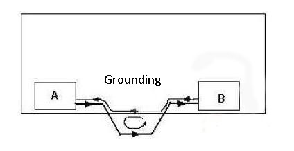 Fig.1. EMI from high-speed line[/caption]
4). Pay attention to the analog signal line. Analog signal line is supposed to be separated from the digital signal line, routing should avoid passing the Aggressor(such as the clock, DC-DC power), and be as short as possible.
4.EMC and signal completeness
1). Terminated resistance. It’s better to terminate with a resistance to the high-speed line or digital signal line with high frequency and long routing.
2). Connect in parallel a capacitor to the input signal line. For the signal line inputted from the interface, it’s better to splice a capacitor in parallel at the point close to the interface. The capacity of the capacitor depends on the signal intensity and frequency(note: if the capacity is too large, it would affect the signal completeness). For the low-speed input signal, such as the keypad input, a 330pF capacitor is available to use, as shown in Fig.2.
[caption id="attachment_4876" align="aligncenter" width="531"]
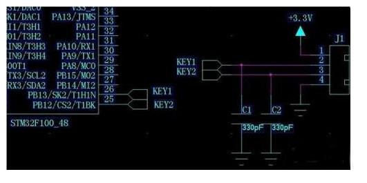 Fig.2 330pF capacitor for keypad input[/caption]
3). The capability of drive. The switch signal with large drive current can be driven with a transistor added; for a bus with a large fanout number, a buffer(such as 74LS224) could be added to drive.
5.Silkscreen
1). Board name, time, PN code.
2). Label. Label the pin of some interfaces or crucial signals.
3). Part Designator. Part designator should be placed properly, dense designator can be placed in groups. Be careful not to place it at the vias.
6. others
Mark point. For the PCB that needs to be assembled by machine, it’s necessary to add 2 to 3 mark points.
 Fig.1. EMI from high-speed line[/caption]
4). Pay attention to the analog signal line. Analog signal line is supposed to be separated from the digital signal line, routing should avoid passing the Aggressor(such as the clock, DC-DC power), and be as short as possible.
4.EMC and signal completeness
1). Terminated resistance. It’s better to terminate with a resistance to the high-speed line or digital signal line with high frequency and long routing.
2). Connect in parallel a capacitor to the input signal line. For the signal line inputted from the interface, it’s better to splice a capacitor in parallel at the point close to the interface. The capacity of the capacitor depends on the signal intensity and frequency(note: if the capacity is too large, it would affect the signal completeness). For the low-speed input signal, such as the keypad input, a 330pF capacitor is available to use, as shown in Fig.2.
[caption id="attachment_4876" align="aligncenter" width="531"]
 Fig.2 330pF capacitor for keypad input[/caption]
3). The capability of drive. The switch signal with large drive current can be driven with a transistor added; for a bus with a large fanout number, a buffer(such as 74LS224) could be added to drive.
5.Silkscreen
1). Board name, time, PN code.
2). Label. Label the pin of some interfaces or crucial signals.
3). Part Designator. Part designator should be placed properly, dense designator can be placed in groups. Be careful not to place it at the vias.
6. others
Mark point. For the PCB that needs to be assembled by machine, it’s necessary to add 2 to 3 mark points.
